


 Tel : +86-592-3926659
 Email : gilia@inthelaboratory.com
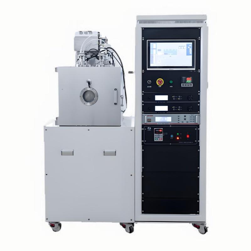
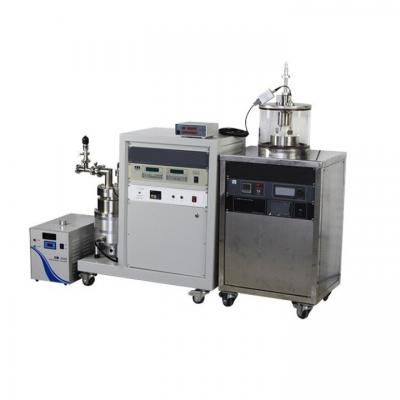
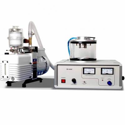
Wafer Sputtering Coater System For Metal/Dielectric Thin Film Deposition In Semiconductor/Optical
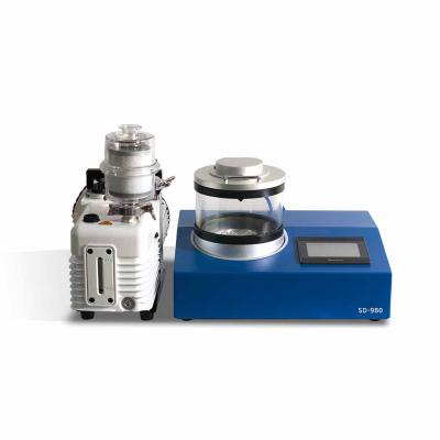
Model: Lith-PD-JS06-Wafer Sputtering Coater System
Product Overview
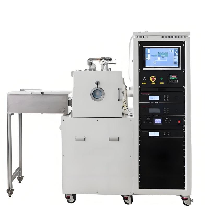
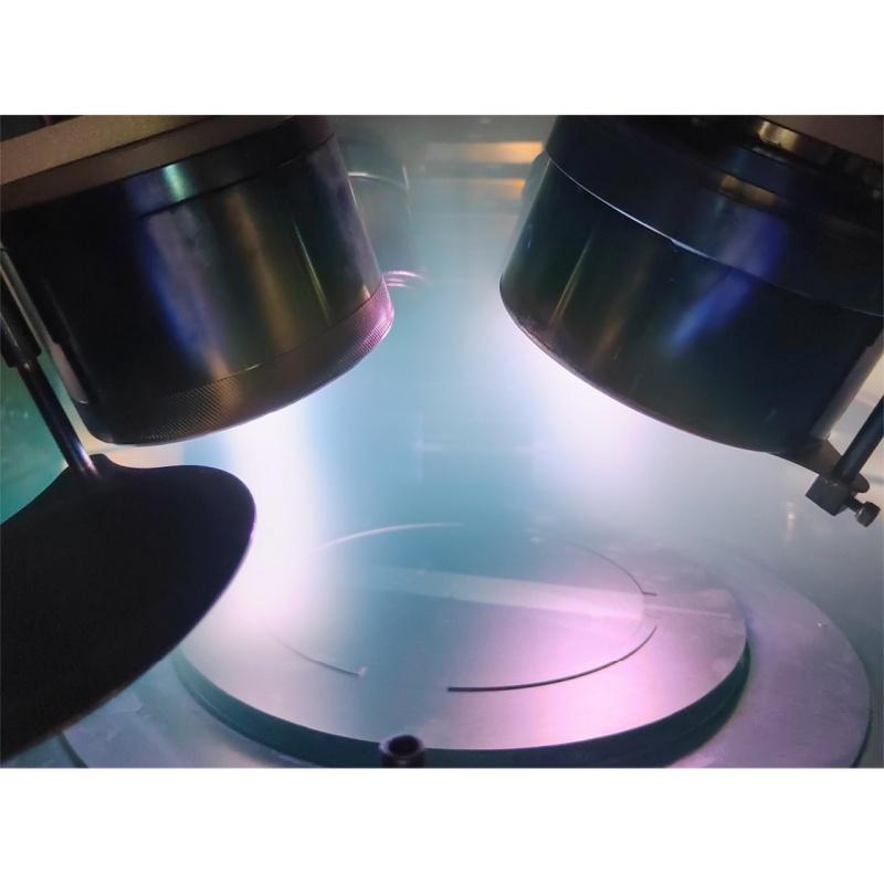
The Lith-PD-JS06 magnetron sputtering system is equipped with multiple sputtering sources, capable of depositing metallic, semiconducting, and dielectric materials. It supports the fabrication of multilayer thin films and co-sputtered alloy films with high precision.
Key Features
· Compact & Integrated Design: Space-saving layout with refined aesthetics, optional sample-loading functionality.
· High Uniformity Coating: Features 4× magnetron sputtering targets (2–4 inches), compatible with 2–8 inch wafers. Substrate holder ensures uniformity within ±3%–5% for 8-inch wafers.
· Flexible Control Options: Siemens PLC + touchscreen (manual/automatic) or PC + PLC full-automatic control.
Technical Specifications
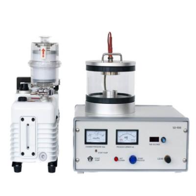
· System Dimensions (L×W×H): 1400 × 1300 × 1900 mm
· Chamber Dimensions (L×W×H): 500 × 500 × 500 mm (PD-500C) / 600 × 600 × 500 mm (PD-600C)
· Substrate Stage: Max heating temperature 500–800°C
· Base Pressure: ≤5 × 10⁻⁵ Pa
· Pumping & Holding: Achieves 8 × 10⁻⁴ Pa within ≤30 min; pressure rise ≤8 Pa over 12 hours.
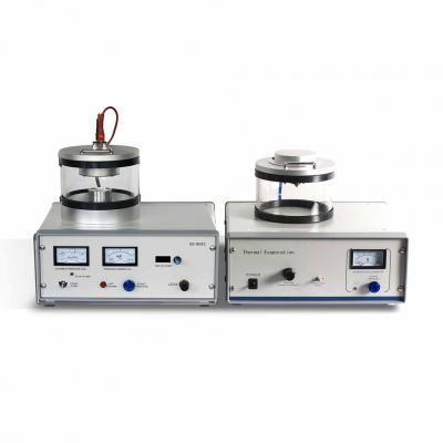
· Target Configuration: 4× sputter guns (2–3 inches or 2–4 inches), coating area 2–6 inches.
Applications & Advantages
Ideal for R&D and small-batch production, this excels in depositing high-quality, uniform thin films for optics, electronics, and functional coatings. Its modular control and excellent temperature/vacuum stability cater to advanced material research and industrial precision demands.
PD-JS06 vs. Conventional Model
|
Feature |
PD-JS05 |
Conventional Systems |
Advantage |
|
Uniformity (8-inch wafer) |
±3%–5% |
±5%–10% or worse |
Higher film consistency for precision applications |
|
System Footprint |
Compact (1400×1300×1900 mm) |
30–50% larger |
Saves lab/cleanroom space |
|
Substrate Heating |
500–800°C |
Typically 300–600°C |
Supports high-temperature depositions (e.g., oxides, nitrides) |
|
Base Vacuum |
≤5×10⁻⁵ Pa |
~1×10⁻⁴ Pa |
Better for reactive sputtering, reduced contamination |
|
Pressure Stability |
≤8 Pa over 12 hours |
Frequent drift (>10 Pa in hours) |
Longer process stability |
|
Control Options |
PLC + Touchscreen or PC + PLC |
Manual or basic PLC |
Flexible automation, better reproducibility |
|
Target Configuration |
4× guns (2–4 inch) |
Often 2–3 guns (2–3 inch) |
Wider material selection, co-sputtering capability |
|
Coating Area |
2–8 inch wafers |
Typically ≤6 inch |
Broader substrate compatibility |
Key Takeaways
· Precision & Consistency: Superior uniformity (±3–5%) vs. conventional (±5–10%).
· Compact & Efficient: 30% smaller footprint without sacrificing performance.
· High-Temp & Vacuum Stability: Enables advanced materials (e.g., optical coatings, semiconductors).
· Automation Ready: PC-controlled processes improve repeatability over manual systems.
Ideal For: R&D labs, semiconductor fabs, and optical coating producers needing high-repeatability, multi-material deposition in a space-efficient design.


 IPv6 network supported