


 Tel : +86-592-3926659
 Email : gilia@inthelaboratory.com
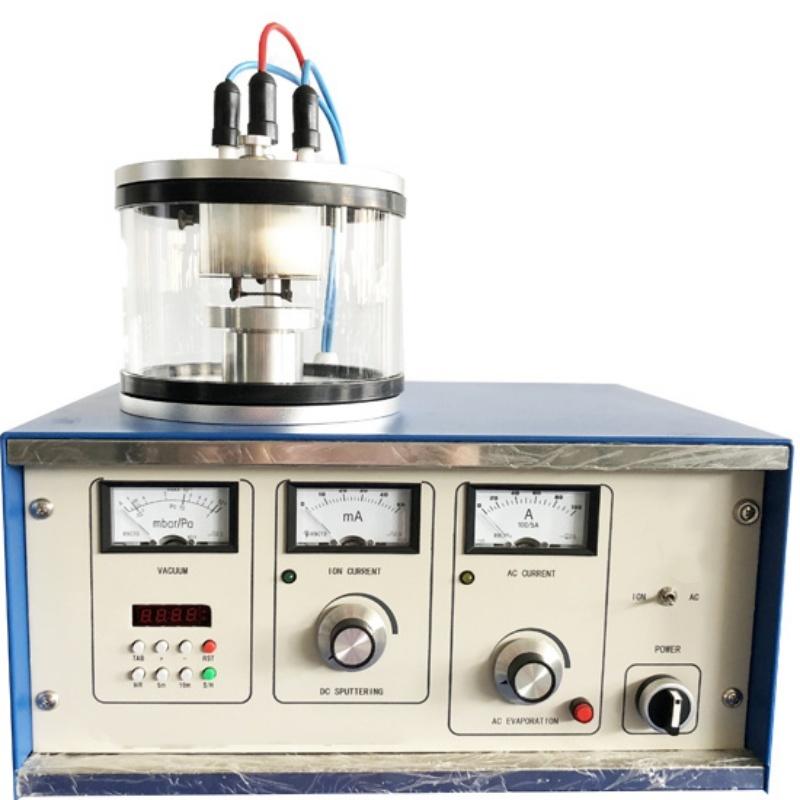
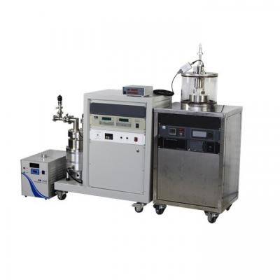
Lab Ion Sputtering & Evaporation PVD Coater Machine for SEM for Glove Box
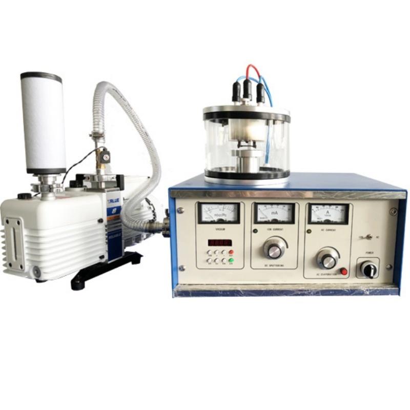
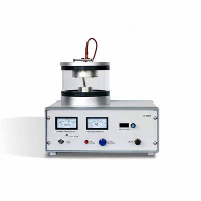
Lith-BY-JS03- Ion Sputtering & Evaporation Coater for SEM
Specification
Integrated with sputtering and thermal evaporation functions, this compact and user-friendly instrument is designed for high-quality thin-film deposition, particularly for SEM sample preparation. It supports multiple metal targets for sputtering and carbon fiber evaporation, offering precise control over coating parameters.
Technical Specifications
|
Parameter |
Value |
|
Dimensions |
305 mm × 400 mm × 390 mm (W×D×H) |
|
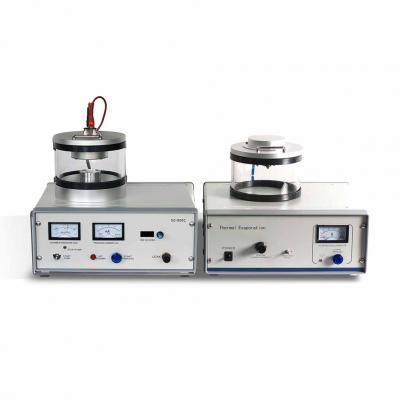
Vacuum Chamber Material |
Borosilicate glass, 160 mm × 110 mm (D×H) |
|
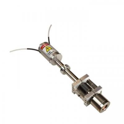
Target (Upper Electrode) |
50 mm × 0.1 mm (D×H) |
|
Sputtering Targets |
Au (standard), optional Ag, Pt, etc. |
|
Target Size |
φ50 mm |
|
Sample Stage |
Compatible with 50 mm/70 mm diameter; customizable |
|
Sputtering Voltage |
0–1600 V (DC), adjustable |
|
Sputtering Current |
0–50 mA |
|
Sputtering Timer |
0–360 s |
|
Carbon Evaporation Current |
0–100 A (AC) |
|
Evaporation Material |
Carbon fiber |
|
Evaporation Voltage |
0–30 V |
|
Evaporation Time |
0–1 s |
|
Gas Inlet Valve |
Compatible with φ3 mm tubing |
|
Process Gases |
Multiple options |
|
Power Supply |
220 V (110 V optional), 50 Hz |
|
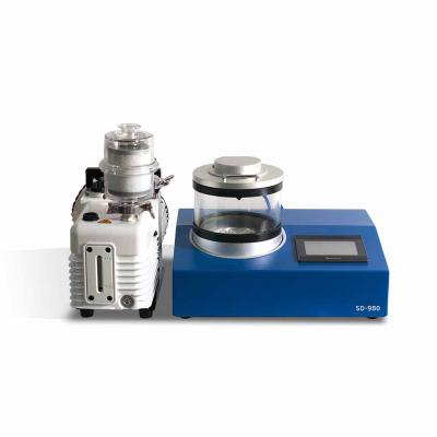
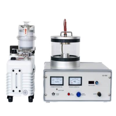
Vacuum Pump |
2L rotary vane pump (VRD-8, domestic) |
Key Features
1. Dual-Function Design
·Combines ion sputtering (Au, Pt, Ag, Cu, etc.) and thermal evaporation (carbon fiber) for versatile applications.
·Ideal for high-resolution microscopy (SEM, TEM, EBSD) requiring ultra-fine carbon films (<1 nm).
2. Precision Control
·Adjustable sputtering current, vacuum pressure, and gas selection to optimize coating rate and particle size.
·Digital timer for reproducible processes.
3. Enhanced Sample Protection
·Conductive coatings eliminate charging effects in non-conductive samples.
·Carbon films protect beam-sensitive materials (e.g., biological/plastic samples) from electron beam damage.
4. Efficiency & Reliability
·Compact footprint with automated vacuum protection to prevent short circuits.
·Uniform film deposition with short processing time.
Applications
· Electron Beam-Sensitive Samples (e.g., polymers, biological tissues): Coating mitigates structural damage.
· Non-Conductive Materials: Metal layers (Au, Pt) dissipate charge, improving SEM imaging.
· Advanced Materials: Enhances conductivity and surface analysis (EBSD, microprobe) for semiconductors/composites.


 IPv6 network supported